Semiconductor manufacturing runs on measurement. Before a wafer moves to the next process step, it often passes through an optical profiler, an inspection system, or a metrology tool that checks step height, film thickness, surface roughness, or defect density down to the nanometer. These systems are only as good as their mechanical platform — and that platform is almost always precision sheet metal.
Behind the optics, sensors, and software of a metrology system sits a structural enclosure that has to do a lot of quiet, unglamorous work: isolate vibration,
block stray light, manage cabling and airflow, and hold every internal component in exact alignment — all while looking clean enough to sit on a fab floor or in an R&D lab next to a customer’s own equipment.
Table of Contents
What Semiconductor Equipment Makers Actually Need from Fabrication
Unlike a general industrial enclosure, a metrology or inspection system chassis has a few requirements that raise the bar on fabrication:
Dimensional stability. Optical measurement systems are sensitiv
e to frame rigidity and flatness. Panels, doors, and structural frames need to hold tight tolerances so they don’t introduce vibration or misalignment that shows up as measurement noise.
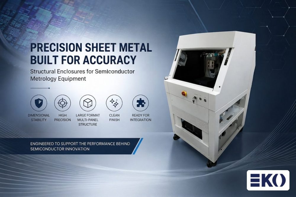
Large-format, multi-panel construction. These systems are often built as tall, modular cabinets — a base structure, a mid-section housing electronics and optics, and a hinged upper enclosure for the measurement head. That means welding, forming, and assembling multiple large panels into one structure that stays square and true.
Clean, presentable finish. Metrology tools are fr
equently installed in cleanroom-adjacent environments or customer-facing labs. Surface finish, edge quality, and paint/coating consistency matter as much as structural integrity — the enclosure is part of the product’s perceived quality.
Access and integration features. Observation windows, cable pass-throughs, ventilation, safety interlocks (E-stop panels, key switches), and swing-out or hinged access panels all have to be engineered into the sheet metal design without compromising rigidity.
Low-to-mid volume, high-mix production. Semiconductor capital equipment isn’t produced at automotive volumes. Fabrication partners need t
o be comfortable with smaller batch sizes, engineering changes between builds, and tight delivery windows tied to customer install schedules.
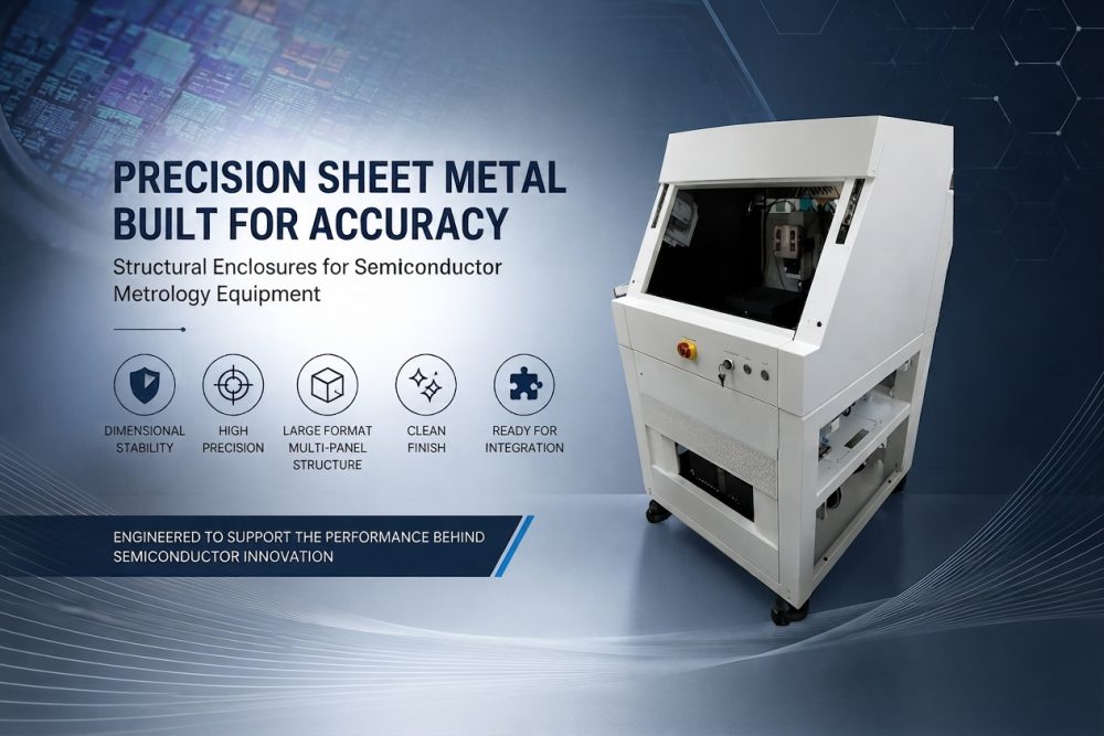
(EKO fabricated this large-format, multi-panel structural enclosure for a leading semiconductor metrology equipment maker.)
Where This Fits in the Broader Supply Chain
As semiconductor and compound semiconductor capacity expands globally — driven by demand across LED, WLCSP/FOWLP packaging, MEMS, PCB, and advanced logic — the equipment makers behind that expansion are increasingly looking outside their home markets for fabrication partners who can match both engineering discipline and cost competitiveness. Southeast Asia, with its established electronics manufacturing base and proximity to the wider semiconductor ecosystem, has become a natural place for that sourcing conversation to happen.
For a fabrication partner, that means being able to support the full build: structural framing, precision panel forming, welding, machining of mounting interfaces, and surface treatment, delivered as a finished, ready-to-integrate enclosure rather than loose parts.

The Common Thread
Whether it’s a data center liquid-cooling manifold or a semiconductor metrology cabinet, the underlying story is the same: as the equipment inside gets more precise, the structure around it has to get more precise too. Sheet metal fabrication that can hold tolerance, stay clean, and scale with a global equipment maker’s build schedule is what turns a good design into a reliable, shippable product.